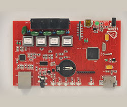
How Does A PCB Assembly Process Work?
In
the modern world, the printed circuit board plays a significant role in
electronic devices. Electronic manufacturers know the importance of these
powerful parts. Though small in size, there is no way you can deny their
contribution to the printed circuit board assembly process. They form the core
of these devices which is a combination of multiple small components. They are
designed with utmost care. Assembling is done in such a way as to reach the
desired outcome as per specifications.
Overview
of the process
There
are numerous stages involved within a printed circuit board. For the
integration of the entire process, all stages need to work cohesively. Develop
an understanding by visiting the site of GREATPCB about PCB
assembly manufacturing
and how all their processes require
careful monitoring. The aim is to derive the product of the highest quality.
·
Solder paste
PCB assembly manufacturing involves
soldering, inspecting, and testing. There has to be an element of compatibility
between each stage, and feedback needs to exist between output and input. In
this way, high quality can be maintained. This step also paves the way for
early detection of issues at an early stage, and steps are accordingly
adjusted. In the initial phase, solder paste has to be applied to those areas
which require solder. These are, in general, component pads, and a solder
screen is used for this purpose. The paste is a blending of grains of solder
along with flux. The process of application of paste is quite similar to that
of any printing process.
·
Pick
and place
The generation of
the solder screen takes place from the files. Holes are present on the solder
pads at specific positions. This step ensures the deposition of solder on
certain solder pads only. The amount to be deposited has to be controlled so
that joints end up with the appropriate amount of solder. The board, along with
the paste, goes through the pick and place process. A machine picks the reels
of components and then places them appropriately on the board. It is the
tension of the paste which helps in holding the various components in position.
As long as there is no jolting, they will stay in place.
·
Further
simplification
In some processes,
glue dots keep the components secure. However, this is undertaken only in cases
of wave soldering. Bear one thing in mind that the presence of glue makes the
repairing work difficult. In some cases, glues are designed purposefully for
degradation in the process. The pick and place process becomes a lot simplified
because the printed circuit board supplies the necessary information.
·
Soldering
machine
The next stage
involves the passing of the process via the soldering machine. In case you are
thinking of using a wave soldering machine, then there is no need to put the
solder paste on the board. However, this method is not widely used, and
instead, reflow soldering procedures are in use nowadays.
·
Inspection
for detection of issues
After the boards go
through the soldering process, the next step is a thorough inspection. Manual
inspection is not possible in all cases due to the involvement of diverse components.
The automatic inspecting helps in the easy detection of issues. The electronic
products are being tested before they make their way outside the factory.
Monitoring of outputs is essential. The objective is attained through the
investigation of issues detected.
Taking
a careful stand
It
is a wise idea to get in touch with a company that is well established in the
industry for printed circuit services. They should have a solid reputation. You
should research intensively on the net and glance through their website. Check
the reviews of past clients thoroughly.


Comments
Post a Comment